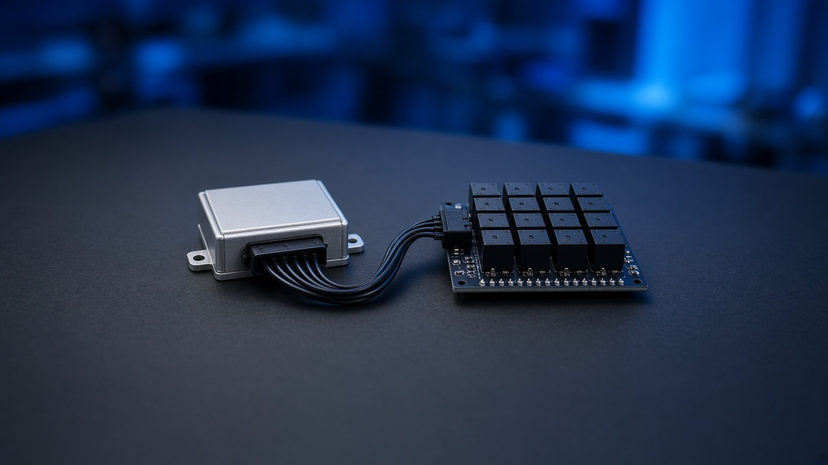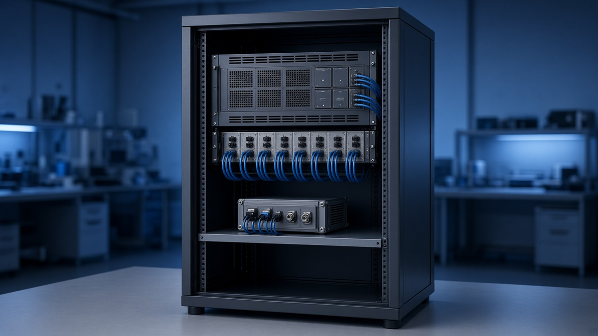


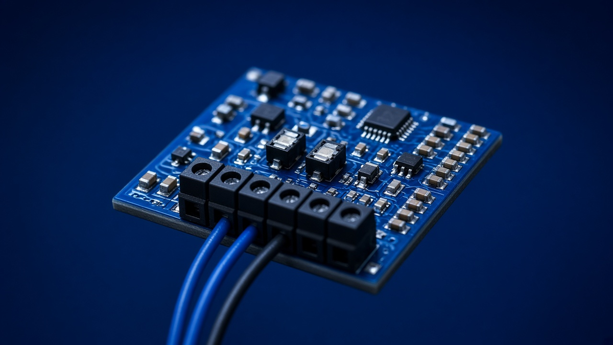
The first time a 24 V wake-up line lands directly on a 5 V acquisition input, the bench usually loses a channel, and sometimes the whole card. Vehicle signals are not logic signals. They are noisy, they swing to battery voltage, they see transients, and sometimes they arrive with the wrong polarity. Between the harness and a logic input, you need a conditioning stage.
This guide walks through the classic series chain, resistor + zener + RC filter, explains what each part does, and shows the calculations that decide whether a design survives on a real bench.
1. The problem: vehicle signals versus logic inputs
1.1 What arrives from the harness
On a validation bench, digital inputs read signals such as ignition, wake-up lines, switch states, or outputs of the unit under test. In a 12 V or 24 V vehicle environment, these signals:
- swing between ground and a supply that is itself variable;
- carry noise picked up along long harness runs;
- can see transients when loads switch, and electrostatic discharge when someone handles connectors;
- can be wired backwards during a test-setup error.
1.2 What the input expects
A logic or DAQ digital input accepts a limited voltage range, has defined high and low thresholds, and has an input impedance that may be high (CMOS) or lower (opto-isolated or current-sinking inputs). Always read these three values in the input’s datasheet before designing anything.
2. The classic chain: series resistor, zener, RC filter
2.1 Described principle diagram
Follow one channel from left to right:
- Input terminal from the harness or breakout box.
- Series resistor R in line with the signal.
- Zener diode Dz from the node after R to ground, cathode on the signal side.
- RC low-pass filter: a capacitor C from the same node (or after a second resistor) to ground.
- Output to the logic or DAQ input, which presents its own load impedance.
2.2 Role of each part
- R limits the current when the zener conducts, and forms the R of the RC filter. Its value sets the trade-off between protection, dissipation and the signal level seen by the load.
- Dz clamps the node to its zener voltage Vz when the input exceeds it, so the logic input never sees more than about Vz. In reverse polarity, it conducts forward and clamps the node to about −0.7 V. Choose Vz below the absolute maximum input voltage of the logic input, not only above its high threshold. A 5.1 V zener protects a 5 V input, not a 3.3 V one; also account for zener tolerance and its soft knee (leakage below Vz).
- C filters fast noise and slows down transients, giving the zener time to react and averaging out short spikes.
3. Calculation 1: dissipation per channel
When the input voltage V exceeds Vz, current flows through R into the zener:
I = (V − Vz) / R
Power splits between the two parts:
- in the resistor: P_R = (V − Vz)² / R
- in the zener: P_Z = Vz × (V − Vz) / R
- total per channel: P ≈ (V − Vz) × V / R
3.1 Worked example
Example, illustrative values, not a product specification. V = 24 V, Vz = 5.1 V, R = 4.7 kΩ.
- I = (24 − 5.1) / 4,700 ≈ 4.0 mA
- P_R = 18.9² / 4,700 ≈ 76 mW
- P_Z = 5.1 × 4.0 mA ≈ 20 mW
- P total ≈ 96 mW per channel
Multiply by the number of channels that can be high at the same time. On a multi-channel enclosure, example: 16 channels × 96 mW ≈ 1.5 W, all inside a closed box. That heat must leave through the enclosure walls. A metal enclosure helps spread it, but the thermal check is needed for each design, at the highest ambient temperature of the test room.
3.2 Choosing the resistor
- Power rating: as a rule of thumb, keep the worst-case P_R at or below about half the rated power, then check it against the manufacturer’s derating curve at the real internal temperature of the enclosure (resistors lose rating above about 70 °C ambient on many datasheets). Apply the same derating logic to the zener’s power at temperature.
- Voltage rating: the resistor must withstand the full transient voltage across it; check the maximum working voltage and the pulse/surge rating from the datasheet.
- Pulse handling: check the pulse rating if transients are expected.
4. Calculation 2: RC cut-off frequency
fc = 1 / (2π × R × C)
4.1 Worked example
Example: R = 4.7 kΩ, C = 10 nF.
fc = 1 / (2π × 4,700 × 10 × 10⁻⁹) ≈ 3.4 kHz. Time constant τ = R × C = 47 µs.
4.2 What it means for your signals
- A slow switch or a wake-up line passes without any issue.
- A PWM signal at a few kHz will be rounded heavily; edges become slow ramps, and the measured duty cycle can shift because the logic threshold is crossed later.
- Edge timing measurement is delayed: rising to 63 % of the final value takes about one τ, and to about 99 % about five τ.
Rule: start from the fastest signal you need to measure, then choose fc well above its useful content. Filter only what you don’t need. If one connector mixes slow states and fast PWM, use different RC values per channel group.
5. Calculation 3: load impedance sets the output level
The logic input is not infinite impedance. With the series R, it forms a voltage divider:
V_out = V_node × R_load / (R + R_load) (in the non-clamped region)
5.1 Worked example
Example: R = 4.7 kΩ, signal 12 V, Vz = 5.1 V.
- Load = 1 MΩ (CMOS input): the zener clamps; V_out ≈ 5.1 V. Good.
- Load = 4.7 kΩ (current-sinking input): the divider gives 12 × 4.7 / (4.7 + 4.7) = 6 V, so the zener still clamps at 5.1 V. Now drop the signal to 8 V, a low-battery case: the divider gives 4 V, below Vz, and possibly close to the input’s minimum high threshold.
A chain designed on paper with “infinite” input impedance may give an undefined logic level on the real input. Always use the input’s specified impedance and its minimum high threshold in the calculation.
6. Fault cases to plan for
| Fault | What happens | Design response |
|---|---|---|
| Reverse polarity | Zener conducts forward, node at about −0.7 V. Example: −24 V through 4.7 kΩ ≈ 5 mA in the zener’s forward direction | Check the input tolerates it; add a series diode if not |
| Overvoltage (sustained) | Zener dissipates continuously | Size R and Dz for the worst sustained voltage |
| Transients | Short high-energy spikes | C + R slow the edge; consider a TVS diode where energy is high |
| ESD at the connector | Very fast discharge | ESD protection close to the connector, short ground path |
| Open input | Floating logic level | Pull-down or pull-up defines the default state |
7. Selection criteria summary
- Input voltage range of the signal, including worst-case and reverse polarity.
- Input thresholds and impedance of the logic/DAQ input.
- Fastest signal to preserve, which fixes the maximum RC.
- Number of channels high at the same time, which fixes enclosure heat.
- Environment: temperature, transients, handling (ESD).
- Traceability: channel numbering identical on the schematic, the enclosure and the wiring list.
8. Common mistakes
- Sizing dissipation for one channel and forgetting the box. Thermal is a whole-enclosure problem.
- Choosing the RC from habit and then wondering why PWM measurements drift.
- Ignoring the load impedance of the acquisition input.
- Forgetting reverse polarity during bench set-up.
- Long ground returns that make the zener clamp relative to the wrong ground.
- No pull resistor on inputs that may be left open.
9. Design checklist
- [ ] Worst-case input voltage and polarity listed per channel.
- [ ] Input thresholds and impedance taken from the datasheet.
- [ ] I, P_R, P_Z calculated per channel at worst case.
- [ ] Total enclosure power checked at maximum ambient temperature.
- [ ] fc checked against the fastest useful signal.
- [ ] Output level checked with the real load impedance.
- [ ] ESD and transient protection placed near the connector.
- [ ] Prototype verified on the bench with the real signal sources before series use.
10. Going further
Conditioning boxes often sit next to a breakout box in the harness path; our guide on specifying breakout boxes covers that side. The timing impact of filtering is discussed in acquisition timing and jitter, and protecting inputs is also a concern in fault injection on harnesses and ECUs. For how such modules are verified at acceptance, see ATP vs QTP.
RAYNOV designs conditioning and protection modules in-house, with electronics in KiCad and mechanics in Autodesk Inventor, as part of custom validation systems. Browse our products.
Need a conditioning stage designed for your signals? Contact our engineering team.
External references (textbook background): RC circuit and Zener diode.